Low-dimensional semiconductors are a focal point of intensive research due to their unique properties, which may yield fascinating new physical phenomena. Nowadays, the large-scale synthesis of 2D materials is an exciting and challenging research area. But unfortunately, the need for large-area 2D films significantly obstructs the development of new technologies based on these novel materials.
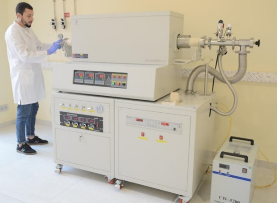
At the School of Applied and Engineering Research Labs, we employ experiments and numerical simulations to study 2D Materials synthesis to develop novel strategies for the large-scale defect-free synthesis of those materials. Chemical vapor deposition (CVD) is the most promising method for synthesizing large-area, high-quality monolayer 2D materials because we can control an extensive range of parameters such as the growth substrate, elemental precursors, temperature, and pressure.
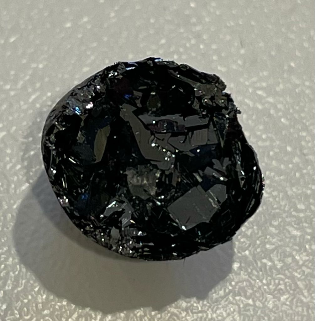
School of Applied and Engineering Research Labs News: We theoretically proved that we can grow phosphorene on a nickel substrate. We successfully synthesized high-quality bulk crystals of 2D materials, including black phosphorous, MoS2, and other transition-metal dichalcogenides (TMDs), while continuing to work on targeting single-crystal growth.
In addition, we are working to scale up the production of high-purity 2D crystals and their atomically thin films to match the current industrial demand for these emerging technologies.
Related publications:
B. D. Tchoffo, I. Benabdallah, A. Aberda, P. Neugebauer, A. Belhboub, A. El Fatimy, Towards large-area and defects-free growth of phosphorene on Nickel, arXiv:2301.06139.


